Recent advancements in photonic devices have opened new avenues for enhancing device efficiency and manufacturability. The introduction of a revolutionary shape optimization method is set to transform metasurface design by addressing the limitations of existing techniques.
This new method not only improves the performance of photonic devices but also allows direct control over fabrication constraints.
Metasurfaces, essential for various applications in optics and photonics, benefit significantly from this shape optimization approach. It considers the interactions between pillars, ensuring that device performance reaches new heights.
Research published in Light: Science & Applications has demonstrated how this technique can lead to high-efficiency metagratings and metalenses, making it applicable across a range of metasurface devices and design objectives.
With the ability to manage shape complexity through Fourier decomposition of boundary gradients, this method opens up possibilities for real-world implementation.
While challenges remain, such as computational intensity and potential trade-offs, the results validate its capability and promise for the future of photonic applications.
The Evolution of Metasurfaces

Metasurfaces represent a groundbreaking advancement in photonics, enabling new functionalities in devices. Understanding their fundamental principles and technological advancements is crucial for appreciating their potential.
Fundamentals of Metasurfaces
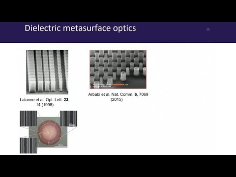
Metasurfaces are engineered materials composed of subwavelength structures known as meta-atoms. These meta-atoms work together to manipulate light in ways that conventional materials cannot.
The design and functionality of metasurfaces rely heavily on the arrangement and geometry of these meta-atoms. Libraries of meta-atoms provide a framework for designing these advanced surfaces, allowing for rapid prototyping and testing.
A key feature of metasurfaces is their ability to control phases, amplitudes, and polarizations of light through precise geometry. This unique capability makes them suitable for applications like imaging devices, sensors, and beam shaping.
Advances in Metasurface Technologies

Recent advancements focus on optimizing the design process, enhancing both efficiency and manufacturability. The new shape optimization methods are particularly noteworthy.
This technique not only builds on traditional approaches but also addresses their limitations. It considers interactions between meta-atoms, improving overall device performance.
There is a strong emphasis on direct control over fabrication constraints, making devices more practical for real-world applications.
For instance, experimental work has shown promising results with high-efficiency metagratings and metalenses, confirming theoretical predictions.
The ability to specify design objectives across various metasurface applications highlights the versatility of this innovation.
The ongoing exploration of these technologies continues to drive progress in the field of photonics.
Optimization and Simulation in Metasurface Design

In metasurface design, optimization and simulation play crucial roles in enhancing efficiency and manufacturability. Different techniques such as shape and topology optimization allow designers to tailor structures for specific applications.
Topology and Shape Optimization Methods
Topology optimization methods focus on the distribution of material within a given design space to maximize performance. They often consider non-local interactions between elements, enhancing the efficiency of metasurfaces.
Shape optimization, on the other hand, refines existing geometries by modifying their boundaries while considering interactions between pillars.
This method has proven advantageous for achieving high performance while maintaining manufacturability.
The innovative shape optimization method discussed in recent research demonstrates significant improvements by controlling surface complexity through Fourier decomposition.
This addresses challenges faced in traditional library-based approaches, enhancing both design flexibility and operational efficiency.
Importance of Electromagnetic Simulation
Electromagnetic simulations are vital for understanding how metasurfaces interact with light.
Both forward and adjoint simulations allow designers to predict the behavior of metasurfaces under different conditions.
Forward simulations provide initial predictions, while adjoint simulations help optimize design parameters more effectively.
This iterative process is essential for refining performance and assessing potential trade-offs.
Accurate simulations also validate the experimental results, ensuring that theoretical designs translate effectively into real-world applications.
By leveraging these simulations, designers can ensure that their structures meet required specifications, thus increasing reliability and effectiveness in practical use.
Innovations in Inverse Design Techniques
Recent advancements in inverse design techniques are reshaping the landscape of metasurface development.
These methods enable designers to define desired optical properties and work backward to achieve them through structured designs.
The innovative approach allows for explicit control of critical design features, such as minimum feature size and gaps between components.
This precision enhances the manufacturability of complex metasurfaces that might previously have been unfeasible.
Recent research highlights the effectiveness of using these inverse design techniques alongside shape optimization methods. This combination offers new pathways to create devices like high-efficiency metagratings and metalenses, significantly boosting their real-world applicability.
Enhancing Photonic Device Efficiency

Improving the efficiency of photonic devices is crucial for advancing applications in communication, imaging, and sensing technologies. This involves assessing key performance metrics, identifying optimization challenges, and addressing manufacturability and practical constraints in design processes.
Key Performance Metrics
In photonic devices, performance metrics like efficiency, bandwidth, and figure of merit are critical.
The efficiency of a metasurface can be defined by how well it converts incoming light into desired outputs. Metrics such as transmission, reflection, and absorption rates determine how much light is effectively utilized.
High-efficiency metasurfaces strive for optimal values in these metrics. The figure of merit quantifies device performance by relating efficiency to size or weight, allowing comparisons across different designs.
By focusing on these metrics, researchers can clearly identify improvements and direct their design efforts more effectively.
Optimization Challenges and Solutions
Optimizing photonic devices faces several challenges, particularly regarding intricate designs and fabrication limits.
The traditional library-based approaches often fall short in dealing with pillar-to-pillar interactions, which are significant for performance.
The new shape optimization method helps overcome these limitations. By using a Fourier decomposition of boundary gradients, the technique can control shape complexity more adeptly.
This mathematical approach allows for precision in feature sizes while addressing performance metrics.
Through experimental validation, designs have shown considerable improvement in efficiency. Yet, it remains vital to balance optimization with the need for practical manufacturing methods, avoiding overly complex designs that could complicate production.
Manufacturability and Practical Constraints
Manufacturability is a significant factor in the realization of high-efficiency metasurfaces.
The new optimization techniques explicitly consider fabrication constraints, such as minimum feature sizes and gaps between structures.
These design parameters directly impact how easily a device can be manufactured. Incorporating these constraints allows engineers to deliver designs that are not only efficient but viable for mass production.
The focus on manufacturability also enhances the applicability of these technologies in real-world settings, aligning theoretical research with practical needs.
Addressing practical limitations while pursuing high performance leads to advancements in the field of photonics.

